Printed Circuit Board (PCB) Explained | How are PCBs made, how do they make modern electronics possible, and is it ever OK to drill through them to mount a cooler...
So, you just bought a shiny new motherboard and after you're done looming and eyeing over the heatsinks that say extreme gamer.
That is designed to look like a battle-ax or whatever you might have noticed all those tiny traces on the board that connect all of your ports headers and sockets together and actually make the board light up and function correctly and although they're not particularly exciting.
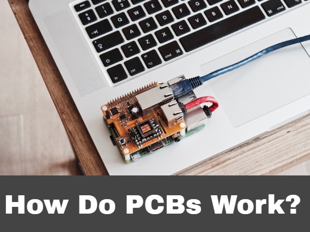
How Do PCBs Work?
Traces on printed circuit boards or PCBs have basically made all of the modern electronics possible. In fact, before they became widespread in the latter half of the 20th century connecting every electrical component inside of an appliance looked a little something like this:
A huge mass of individual wires. This is actually a look inside of a TV from 1948 and you imagine trying to build a computer or even buy a flat panel TV if you had to deal with that!
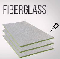
Fortunately, the idea of embedding wires in a flat piece of fiberglass really took off as the years went by making it possible to fit a PC in a backpack instead of a giant cabinet, but how exactly then do they pack so many important connections in such a small space.
The process is actually somewhat similar to how CPUs are manufactured? Which you can learn more about in this Article
I'll be it add a bit of less complicated scale.
- Slices of fiberglass are stacked together and treated with a resin makes them stick to each other to make one solid slab.
- Then layers of copper are applied to both sides and coat it in a chemical called photoresist.
- After this a pattern that matches up exactly to the traces that are supposed to go on the board is placed on top.
- Then the whole thing is exposed to UV light.
- The board is then washed which well washes away the uncovered areas leaving tracks of copper these tracks serve as a base for how the PCB will ultimately look after a couple of more steps including:
- Catching additional copper and more washing but keep in mind that this process is often done in layers which is why it's a terrible idea to try and drill through your motherboard
If you're having trouble mounting a cooler to it. The Internet has more than a few tales of people that tried to do this only to find out that their board didn't work at all.
Afterward because they drilled in the middle of traces that were visible from the outside but went right through ones that were inside of it but that isn't to say that boards don't get drilled at all during manufacturing.
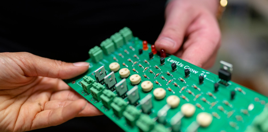
At the factory boards not only get mounting holes drilled through them for whatever form factor they happen to fit in but they also get small holes to accommodate connections for small electrical components like chips capacitors and resistors as well as tiny interconnects between the different layers of copper traces.
So after things like PCI Express slots heat sinks and CPU sockets are mounted or soldered to the board it's basically finished.
But since a PCB is just a collection of electrical connections on some kind of a substrate you don't actually need any fancy manufacturing processes to make a simple one.
In fact, you can even buy markers that will dispense electrically conductive ink onto special paper so you can literally draw your own working PCB (Pretty cool).
But given the inherent complexity in manufacturing something like an ATX motherboard. I wouldn't count on being able to make your own one of those and maybe stick to you know making LED art that you can stick to your refrigerator.
Printed Circuit Board Explained! || How Do PCBs Work?
I hope you enjoyed the article and it increases your knowledge about PCB Boards. Please like MY FACEBOOK PAGE for more information related to PCB Layout designing (Circuit2PCB).
You can message me directly. I will try my best to help you as much as I can with my PCB skills.
You can also see my Latest PCB design projects.
My Freelance Profile: https://www.fiverr.com/circuit2pcb
About Me:
"Electronics Engineer, Expert 3D PCB Layout Designer"
My name is Ahsan Mehmood Awan and I am from Pakistan. Since Summer 2020, I am a graduate Electrical Engineer with the main focus on Electronics Engineering. I am fluent in English (mother tongue) as well as in Urdu and Punjabi. I am mainly working as a helper in electrical/electronics courses, calculus, circuit analysis, problem-solving, power electronics, linear algebra, mathematics, PCB design, simulation, c++ programming, and much more related to my field.
I have 5 Years+ Experience in MATLAB coding, Circuits Design, PCB Design, c++ programming coding, Microsoft Office Word, Multisim Circuit Simulation, Proteus, Vivado FPGA, Fritzing breadboard, EDA PCB, etc
I have been offering my electrical/electronics services on Fiverr as a freelancer for more than 2 years. I am currently realizing my studies at UET TAXILA university for specialization.
I'm also a Blogger & Wordpress developer. I enjoy my life very well, my main goal is to make my customer happy with my quality work. You can easily inbox me whenever you need help related to electrical/electronics engineering.
Regards,
Circuit2Pcb
Thanks for your time!
- Related Tags: printed circuit board,circuit board,printed circuit boards,how to make a printed circuit board,printed circuit board manufacturing,diy printed circuit board,printed circuit board design,printed circuit board manufacturing process,how to design printed circuit board,what is printed circuit board,printed circuit board fabrication,circuit,electronic circuit,printed circuit board explanation,3d printed circuit board,printed circuit board meaning,how to make printed circuit board
Printed Circuit Board Explained! || How Do PCBs Work?
 Reviewed by Ahsan Mehmood Awan
on
May 25, 2020
Rating:
 Reviewed by Ahsan Mehmood Awan
on
May 25, 2020
Rating:


No comments: